There’s something happening to the IT industry, that maybe has not happened in a couple of decades or so but hardware innovation is back. We’ve been covering bits and pieces of it in our hardware vs software innovation series (see Open source ASiCs – HW vs. SW innovation [round 5] post).
But first please take our new poll:

Hardware innovation never really went away, Intel, AMD, Apple and others had always worked on new compute chips. DRAM and NAND also have taken giant leaps over the last two decades. These were all major hardware suppliers. But special purpose chips, non CPU compute engines, and hardware accelerators had been relegated to the dustbins of history as the CPU giants kept assimilating their functionality into the next round of CPU chips.
And then something happened. It kind of made sense for GPUs to be their own electronics as these were SIMD architectures intrinsically different than SISD, standard von Neumann X86 and ARM CPUs architectures

But for some reason it didn’t stop there. We first started seeing some inklings of new hardware innovation in the AI space with a number of special purpose DL NN accelerators coming online over the last 5 years or so (see Google TPU, SC20-Cerebras, GraphCore GC2 IPU chip, AI at the Edge Mythic and Syntiants IPU chips, and neuromorphic chips from BrainChip, Intel, IBM , others). Again, one could look at these as taking the SIMD model of GPUs into a slightly different direction. It’s probably one reason that GPUs were so useful for AI-ML-DL but further accelerations were now possible.

But it hasn’t stopped there either. In the last year or so we have seen SPUs (Nebulon Storage), DPUs (Fungible, NVIDIA Networking, others), and computational storage (NGD Systems, ScaleFlux Storage, others) all come online and become available to the enterprise. And most of these are for more normal workload environments, i.e., not AI-ML-DL workloads,

I thought at first these were just FPGAs implementing different logic but now I understand that many of these include ASICs as well. Most of these incorporate a standard von Neumann CPU (mostly ARM) along with special purpose hardware to speed up certain types of processing (such as low latency data transfer, encryption, compression, etc.).
What happened?
It’s pretty easy to understand why non-von Neumann computing architectures should come about. Witness all those new AI-ML-DL chips that have become available. And why these would be implemented outside the normal X86-ARM CPU environment.
But SPU, DPUs and computational storage, all have typical von Neumann CPUs (mostly ARM) as well as other special purpose logic on them.
Why?
I believe there are a few reasons, but the main two are that Moore’s law (every 2 years halving the size of transistors, effectively doubling transistor counts in same area) is slowing down and Dennard scaling (as you reduce the size of transistors their power consumption goes down and speed goes up) has stopped almost. Both of these have caused major CPU chip manufacturers to focus on adding cores to boost performance rather than just adding more transistors to the same core to increase functionality.
This hasn’t stopped adding instruction functionality to each CPU, but it has slowed considerably. And single (core) processor speeds (GHz) have reached a plateau.
But what it has stopped is having the real estate available on a CPU chip to absorb lots of additional hardware functionality. Which had been the case since the 1980’s.
I was talking with a friend who used to work on math co-processors, like the 8087, 80287, & 80387 that performed floating point arithmetic. But after the 486, floating point logic was completely integrated into the CPU chip itself, killing off the co-processors business.
Hardware design is getting easier & chip fabrication is becoming a commodity
We wrote a post a couple of weeks back talking about an open foundry (see HW vs. SW innovation round 5 noted above)that would take a hardware design and manufacture the ASICs for you for free (or at little cost). This says that the tool chain to perform chip design is becoming more standardized and much less complex. Does this mean that it takes less than 18 months to create an ASIC. I don’t know but it seems so.
But the real interesting aspect of this is that world class foundries are now available outside the major CPU developers. And these foundries, for a fair but high price, would be glad to fabricate a 1000 or million chips for you.
Yes your basic state of the art fab probably costs $12B plus these days. But all that has meant is that A) they will take any chip design and manufacture it, B) they need to keep the factory volume up by manufacturing chips in order to amortize the FAB’s high price and C) they have to keep their technology competitive or chip manufacturing will go elsewhere.
So chip fabrication is not quite a commodity. But there’s enough state of the art FABs in existence to make it seem so.
But it’s also physics
The extremely low latencies that are available with NVMe storage and, higher speed networking (100GbE & above) are demanding a lot more processing power to keep up with. And just the physics of how long it takes to transfer data across a distance (aka racks) is starting to consume too much overhead and impacting other work that could be done.
When we start measuring IO latencies in under 50 microseconds, there’s just not a lot of CPU instructions and task switching that can go on anymore. Yes, you could devote a whole core or two to this process and keep up with it. But wouldn’t the data center be better served keeping that core busy with normal work and offloading that low-latency, realtime (like) work to a hardware accelerator that could be executing on the network rather than behind a NIC.
So real time processing has become faster, or rather the amount of time to execute CPU instructions to switch tasks and to process data that needs to be done in realtime to keep up with faster line speed is becoming shorter.
So that explains DPUs, smart NICS, DPUs, & SPUs. What about the other hardware accelerator cards.
- AI-ML-DL is becoming such an important and data AND compute intensive workload that just like GPUs before them, TPUs & IPUs are becoming a necessary evil if we want to service those workloads effectively and expeditiously.
- Computational storage is becoming more wide spread because although data compression can be easily done at the CPU, it can be done faster (less data needs to be transferred back and forth) at the smart Drive.
My guess we haven’t seen the end of this at all. When you open up the possibility of having a long term business model, focused on hardware accelerators there would seem to be a lot of stuff that needs to be done and could be done faster and more effectively outside the core CPU.
There was a point over the last decade where software was destined to “eat the world”. I get a lot of flack for saying that was BS and that hardware innovation is really eating the world. Now that hardtware innovation’s back, it seems to be a little of both.
Comments?
Photo Credits:
- Cerebras chip, Cerebras (see SC20 post)
- Mythic architecture, Mythic computing (see AI at the edge post)
- TPU2-iot, Google (see TPU post)
- 130nm layouts (see Open source ASICs post)
- Moore’s law chart – wikipedia, By Max Roser – https://ourworldindata.org/uploads/2019/05/Transistor-Count-over-time-to-2018.png, CC BY-SA 4.0, https://commons.wikimedia.org/w/index.php?curid=79751151
 Was at
  During their development activity they tested various configurations. At the start of their development they used a Windows Server with their NVMeoF target device driver. With this configuration and on a bare metal server, they found that they could max out the Optane SSD at 550K 4K random write IOPs at 0.6msec to a single Optane drive.
 NetApp announced this week that their latest generation AFF (All Flash FAS) systems will support FC NVMeoF. We asked if this was just for NVMe SSDs or did it apply to all AFF media. The answer was it’s just another host interface which the customer can license for NVMe SSDs (available only on AFF F800) or SAS SSDs (A700S, A700, and A300). The only AFF not supporting the new host interface is their lowend AFF A220.
 They also christened their new Data Visualization Center (DVC) and we had a multi-course meal at the Bistro at the center. The DVC had a wrap around, 1.5 floor tall screen which showed some of NetApp customer success stories. Inside the screen was a more immersive setting and there was plenty of VR equipment in work spaces alongside customer conference rooms.
 The hardware
 With Axellio using all NVMe SSDs, we expect high IO performance. Further, they are measuring IO performance from internal to the CPUs on the Axellio server nodes. X-IO says the Axellio can hit >12Million IO/sec with at 35µsec latencies with 72 NVMe SSDs.
 Other sessions at X-IO include: Richard Lary, CTO X-IO Technologies gave a very interesting presentation on an mathematically optimized way to do data dedupe (caution some math involved); Bill Miller, CEO X-IO Technologies presented on edge computing’s new requirements and Gavin McLaughlin, Strategy & Communications talked about X-IO’s history and new approach to take the company into more profitable business.
 At
At  Elastifile’s architecture supports accessor, owner and data nodes. But these can all be colocated on the same server or segregated across different servers.
 Metadata operations are persisted via journaled transactions and which are distributed across the cluster. For instance the journal entries for a mapping data object updates are written to the same file data object (OID) as the actual file data, the 4KB compressed data object.
 There’s plenty of discussion on how they manage consistency for their metadata across cluster nodes. Elastifile invented and use Bizur, a key-value consensus based DB. Their chief architect Ezra Hoch (
 We, the industry and I, have had a long running debate on whether hardware innovation still makes sense anymore (see my Hardware vs. software innovation – rounds
  DSSD required specialized hardware and software in the client or host server, specialized cabling between the client and the DSSD storage device and specialized hardware and flash storage in the storage device.
 There’s got to be a way to more quickly fix ASIC and other hardware errors. Yes some hardware fixes can be done in software but occasionally the fix requires hardware changes. A quicker hardware fix approach should help.
 At
At  No. The target storage system used during their demo consisted of:
 During the 4.5M IO/sec random read benchmark, the storage target CPU was at 0.3% busy and the highest consuming process on the target CPU was the Linux “Top” command used to display the PS status.
 Read an article the other day in Ars Technica (
 (
( What about DRAM replacement?
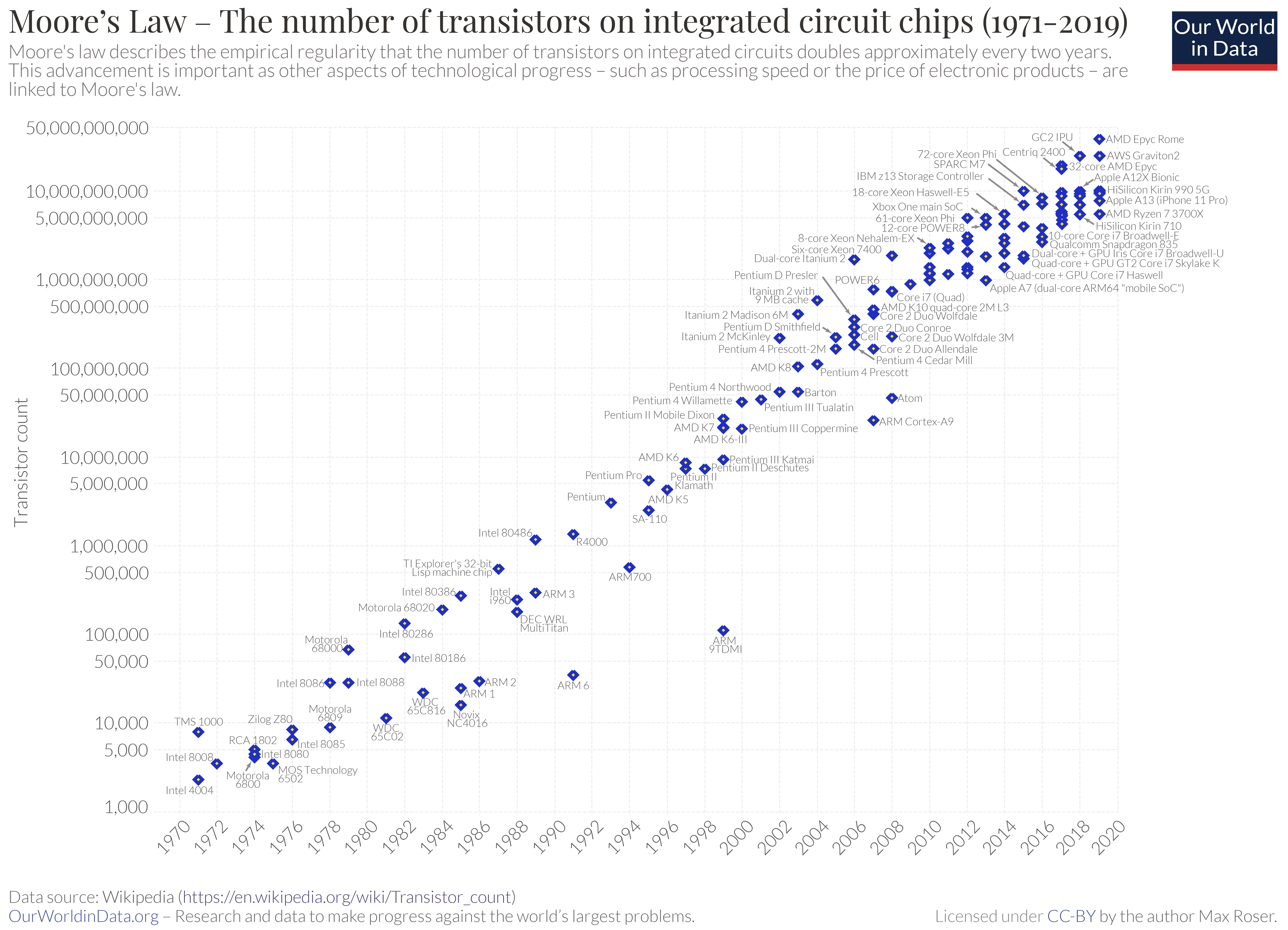